This Certificate Comes with TSMC’s Guarantee! NUK and TSMC Launch Semiconductor Program to Cultivate Advanced Process Talent in Southern Taiwan

【Text : Wan-Chen Hung, Special Assistant, Advanced Packaging Integrated Technology Center; Edited by: Public Affairs Section】
【Promotion of the United Nations Sustainable Development Goals (SDGs) series】
2025-07-15 This certificate comes with TSMC’s guarantee! The National University of Kaohsiung (NUK) has partnered with Taiwan Semiconductor Manufacturing Company (TSMC), the world’s leading semiconductor foundry, to officially launch the TSMC Semiconductor Program for talent cultivation. Students who complete the program will receive a certificate issued by TSMC, effectively linking them to the southern Taiwan technology cluster and supplying the nation’s semiconductor industry with highly skilled technical talent.
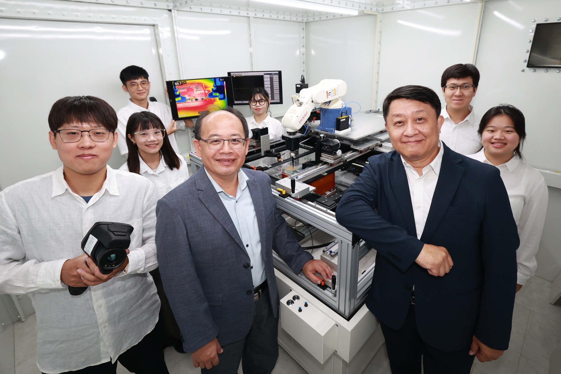
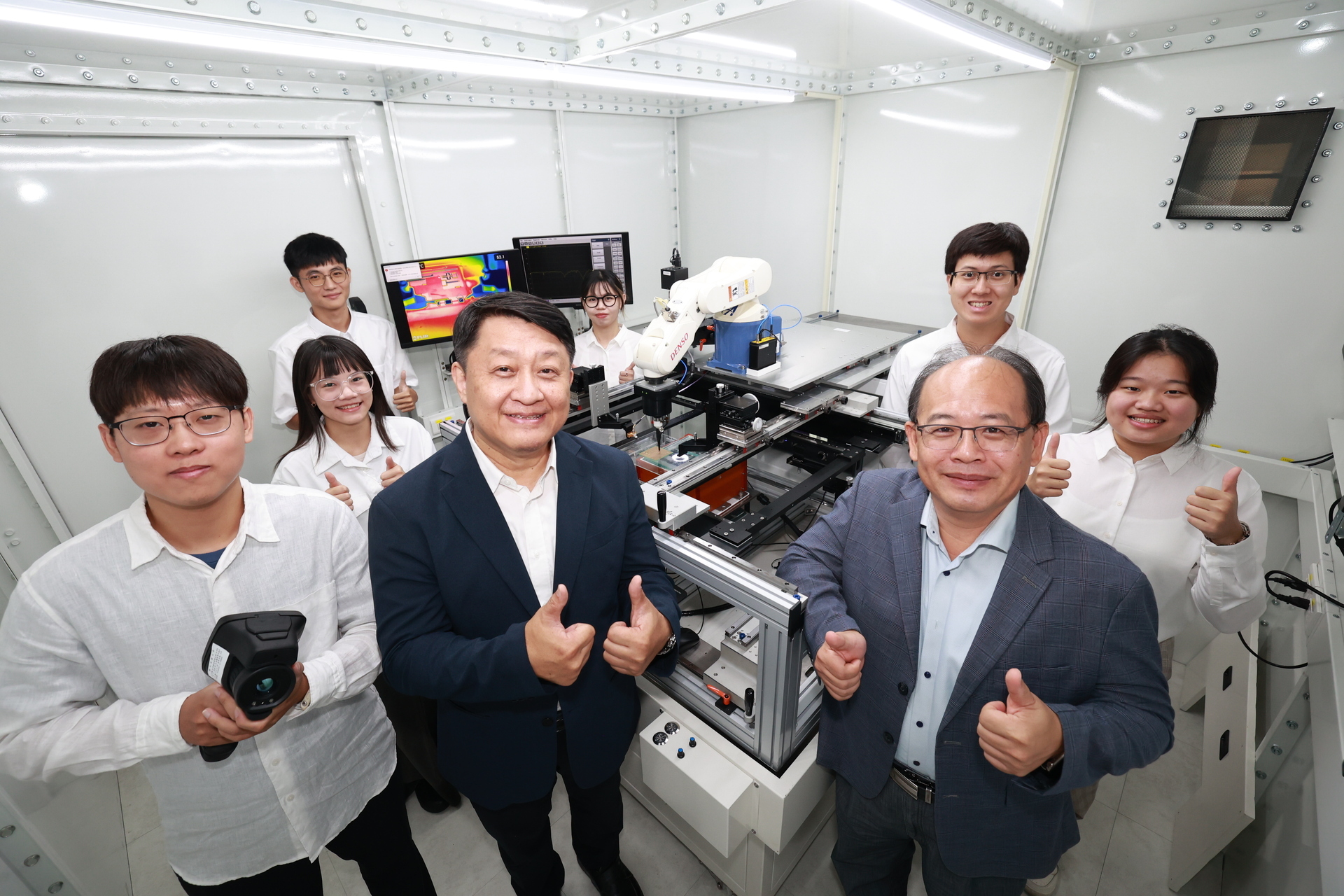
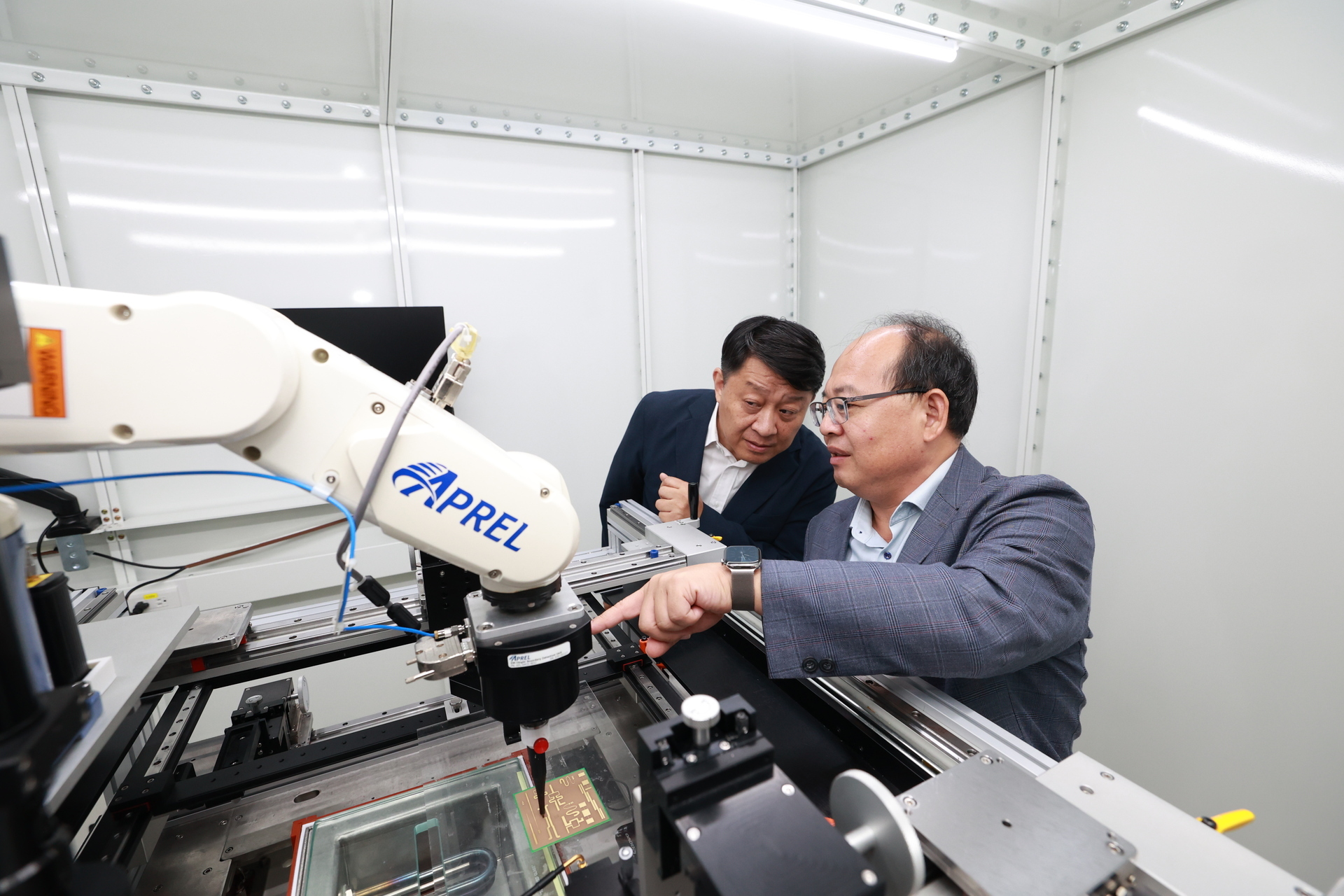
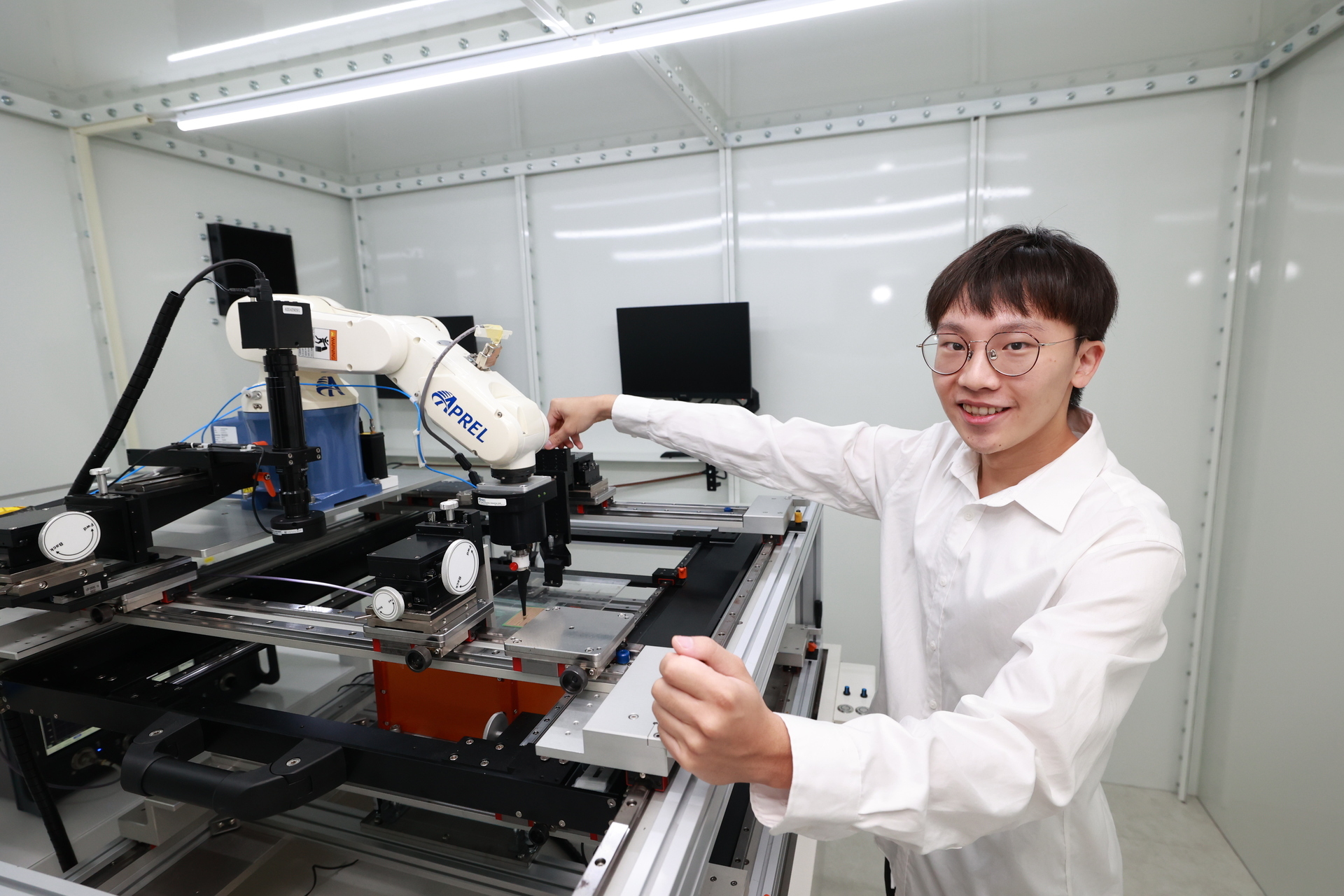
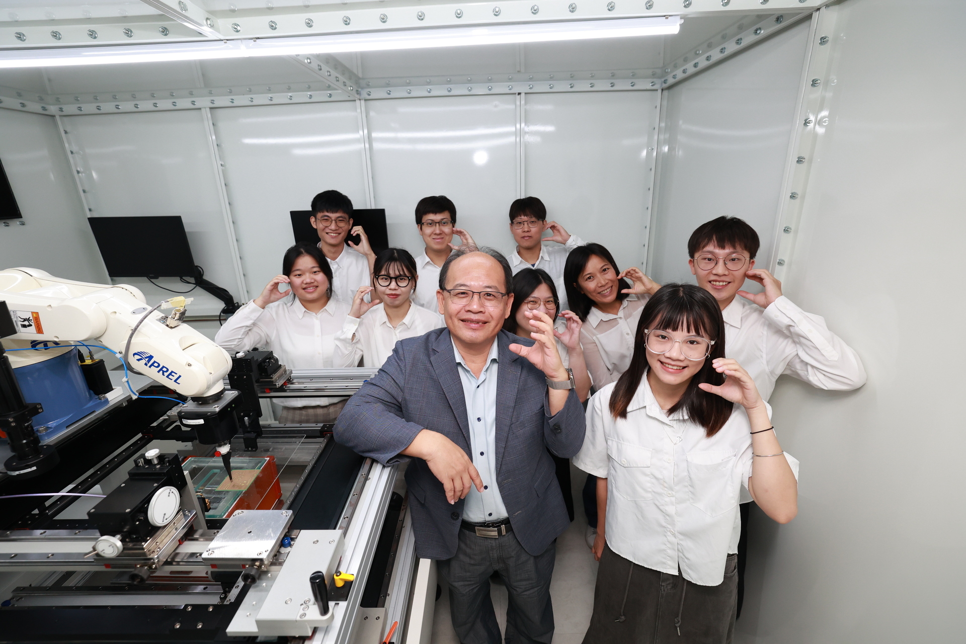
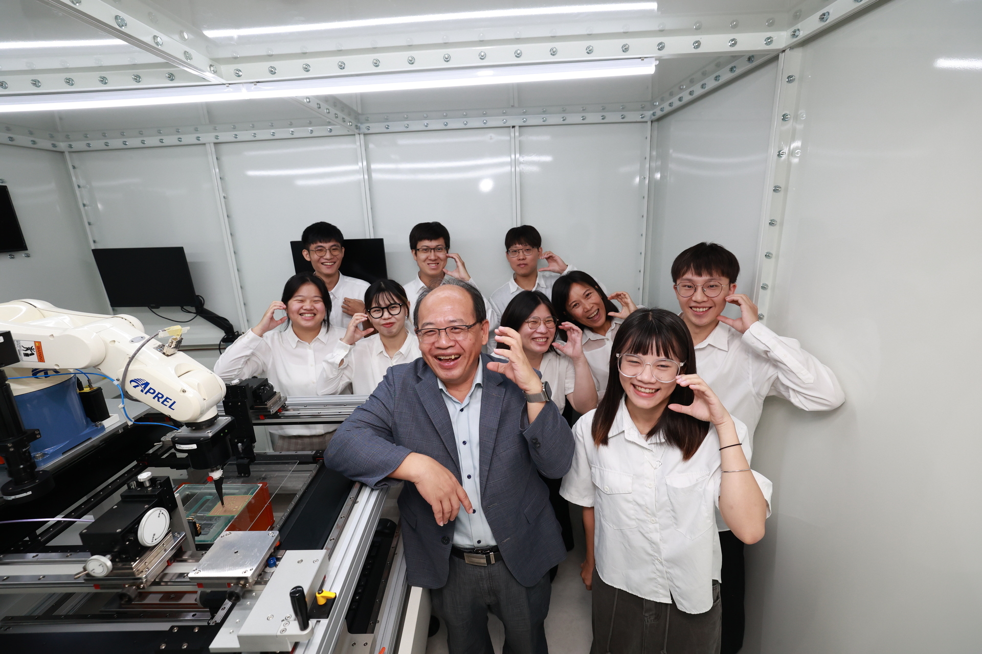
NUK President Chen Chi-Jen noted that the university is located at the heart of the southern Taiwan Semiconductor S Corridor, adjacent to the Nanzih Technology Industrial Park and Qiaotou Science Park, offering both geographic and industry-academia linkage advantages. Since 2006, NUK has offered the “Semiconductor and Optoelectronic Process Program,” building extensive teaching and practical experience, and established the Advanced Packaging Integration Technology Center to continue deepening expertise in packaging, assembly, and process development—laying a solid foundation for southern Taiwan’s semiconductor growth.
President Chen explained that this new program is coordinated by the Office of the Academic Vice President and supported by the Office of Research and Development, integrating teaching resources from eight departments and graduate institutes: Electrical Engineering, Chemical and Materials Engineering, Civil and Environmental Engineering, Computer Science and Information Engineering, Applied Chemistry, Applied Physics, Applied Mathematics, and Statistics. The curriculum is designed in line with a training blueprint provided by TSMC, and includes three tiers—Required Courses, Core Electives, and Professional Electives—with a minimum requirement of 11 courses. Vice President for Research and Development Wu Sung-Mao has actively engaged in multiple discussions with TSMC to finalize course content and collaboration details.
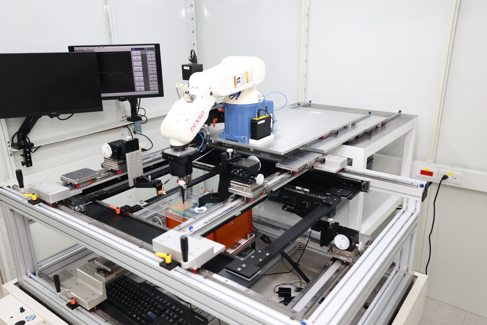
Academic Vice President Chuang Hsiu-Hui highlighted that TSMC’s current focus areas—Chip-on-Wafer-on-Substrate (CoWoS), System-on-Integrated-Chip (SoIC), and Chiplets advanced packaging architectures—are areas where NUK has strong teaching and R&D foundations. The program integrates fundamental courses in electronics, circuit design, device physics, analytical chemistry, and process technology, extending into electives such as integrated circuit design, materials analysis, optoelectronic applications, and heterogeneous integration testing and packaging. The curriculum retains NUK’s specialized strengths in process control and advanced packaging, enabling students to build comprehensive semiconductor engineering competencies and achieve a dual-track goal of technical depth and cross-disciplinary integration. The ultimate aim is to cultivate T-shaped talent with expertise in process R&D, testing and packaging engineering, and 3D integration design—aligned with both industry technology trends and national strategic needs.
The course modules have been fully integrated and internally reviewed, and the program has been formally submitted for evaluation under the TSMC Semiconductor Talent Cultivation Project. Upon approval, the courses will be progressively opened for NUK students to enroll. Future plans include the introduction of a hybrid teaching platform combining remote hands-on training, corporate case studies, and AI simulation applications—creating a more industry-ready and adaptive learning environment.
#SDG4 #SDG8 #SDG9 #SDG17 @Advanced Packaging Integration Technology Center & Research